Intel Meteor Lake Architecture Deep Dive: Tiles, New Cores And AI For All
Intel’s Meteor Lake architecture for mobile PCs will be arriving soon and to say that Meteor Lake is the most important shift in Intel’s design and manufacturing approach could be an understatement. In fact, Intel has called Meteor Lake the largest architecture shift in the last 40 years, and it will influence designs for a decade to come.
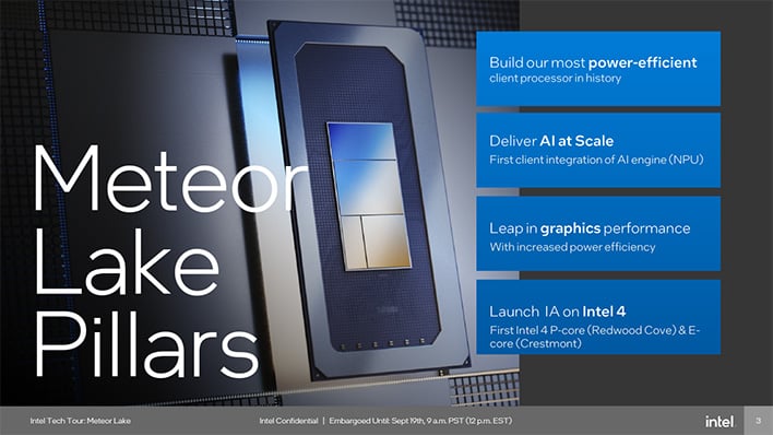 Intel has outlined four key pillars for Meteor Lake. First, it is designed to be the most power efficient client processor in the company's history. Second, it will be Intel’s first consumer CPU to deliver a dedicated AI engine at scale. Third, Intel is targeting a leap in graphics performance along with power efficiency. Finally, it will be the debut of the Intel 4 process, at least in part.
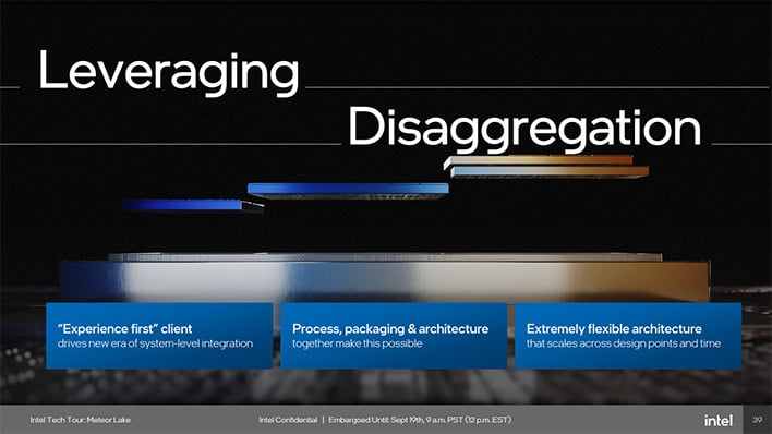 Meteor Lake is the company’s first truly disaggregated consumer chip, and its development has been challenging. Disaggregation means that rather than using a single monolithic die to house the CPU cores, integrated GPU, I/O features, and other uncore “stuff,” various engines are instead broken out into multiple chiplets that Intel calls Tiles. This is an attractive approach for many reasons. Dies can only be made so large, while remaining economically and physically feasible. Current processes are limited by reticle sizes during the lithography etching, but there’s more to consider than just this (more or less) hard limit. A larger die not only has more “wasted” space around the edges of a round 300mm wafer, but is also more likely to have debilitating defects, and that has a direct negative impact on yields. Smaller chips let manufacturers extract more from each wafer, maximizing the potential value of each.
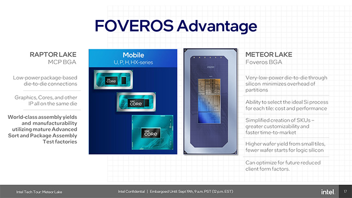
Breaking up a design into smaller chiplets has its own drawbacks, of course. Packaging it all together becomes a lot more complex, no matter how you slice it. If we disregard 3D V-Cache for a moment, AMD arranges chiplets around each other on a single PCB for its processors, whereas Intel opts to stack silicon directly using its Foveros and Embedded Multi-die Interconnect Bridge (EMIB) technologies. Foveros and EMIB are similar, but distinct advanced packaging techniques that Intel has been using in some products for a few years now.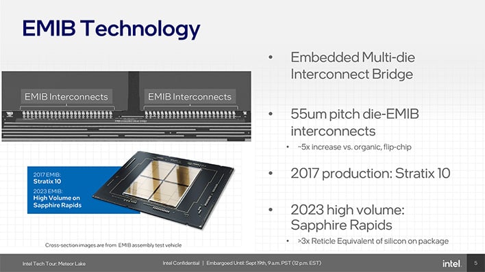
EMIB debuted first in 2017 in the Stratix 10. This was a field-programmable grid array (FPGA) chip, but the technology has matured into high volume production and is used by Sapphire Rapids today. EMIB uses 55um pitch interconnects to mount die atop the embedded silicon bridge.
Foveros allows for active-on-active “3D” stacking with greater complexity. Foveros was introduced with Lakefield in 2020, where it allowed Intel to layer a compute die with PoP DRAM on top of a base die that is then mounted on the package substrate.
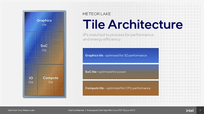 Meteor Lake’s design uses four distinct tiles riding atop a base tile assembled using Foveros 3D packaging technology. These are the Compute tile, GPU tile, SOC tile, and IO tile respectively, which gives some insight into the core function of each. There are certainly some nuances to this though, so lets quickly go over the high-level attributes of each before we dig deeper.
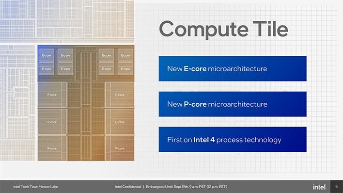
The Compute tile is where most of the processors cores reside. Most you may ask? We’ll get to that. The Compute tile features a mix of the P-cores and E-cores we’re used to from Alder Lake and Raptor Lake, with some microarchitectural improvements. The Compute tile is built using the Intel 4 process node and is actually the only tile in the system directly fabbed by Intel.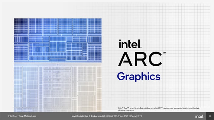
The GPU tile is next up. As expected, this contains Intel’s Arc Graphics architecture, specifically Xe-LPG. This is fabbed by TSMC on its N5 process and designed to deliver an approximate 2x performance per watt improvement over the 12th gen Xe graphics. The Graphics tile does not house the Media Engine, though. That has been separated out to reside on the SOC tile, along with the display interfaces.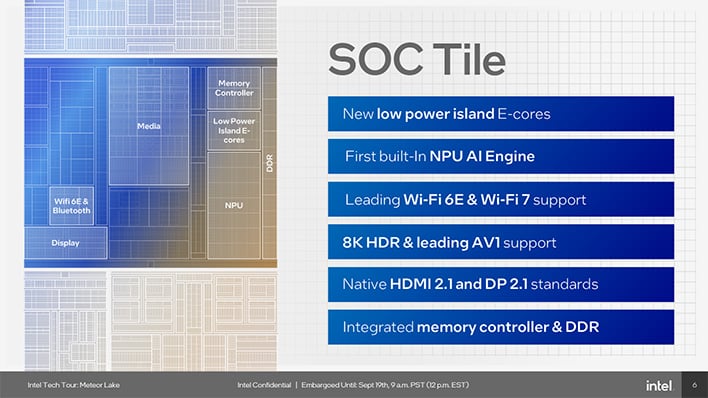 The SOC tile is the home of a wide variety of functions across two scalable fabrics. The North side features the Network on Chip (NOC) fabric linking high performance devices while the South side has an efficient PCIe-based IO fabric, with an IOC bridge linking the two. Beyond connectivity and the media/display engines, it also houses the NPU AI engine, memory controller, and two special E-Cores of its own. The IO tile acts as an extension of the SOC tile’s IO fabric and both are fabbed using TSMC’s N6 process.
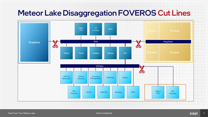 As we dive deeper into the architecture, let’s start with the SOC tile. It sits at the center of everything and links directly to the Compute, Graphics, and IO tiles. In effect, these linkages are where “cuts” were made to break out from a traditional monolithic die approach. If we back up for a moment, SOC architectures are deceptively complex, and impacts fab initiated processes and the ability to ramp new nodes. Breaking the chip up like this frees the architects to work with IP appropriate manufacturing processes. The disaggregation ensures that Compute Tile of future products, for example, can quickly ramp to Intel 3 and beyond while the other parts of the SOC, which may not benefit much from more advanced process nodes, can advance at a slower rate.
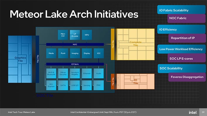 Meteor Lake's architectural shifts and design philosophies were driven by a few initiatives. The first was to implement the NOC fabric to meet the demands of high-performance devices, while letting the IO fabric provide efficient access for lower power uses. To improve IO efficiency, Intel moved graphics to its own tile, but kept the media and display blocks with the SOC tile. Finally, the power management system needed to be scalable, with control over each tile and even subsystems within the tiles. As an example, this allows the PMC for the Compute Tile to be tuned to the number of P- and E-cores available, while the central PMC on the SOC tile is agnostic to the Compute Tile configuration.
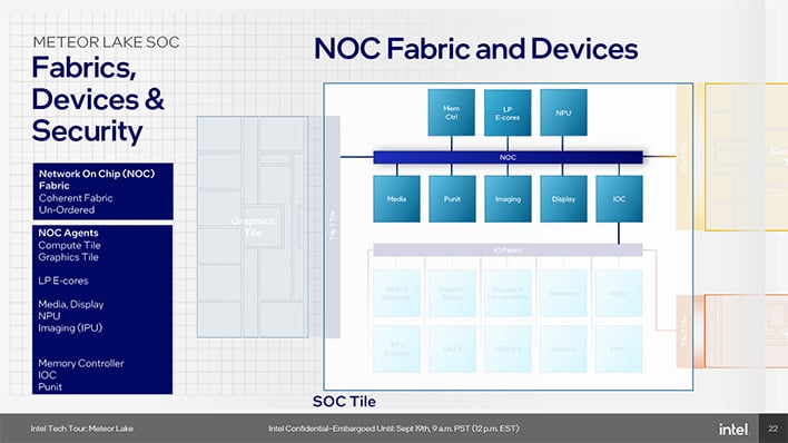 The “North” NOC fabric is a cache-coherent, un-ordered interface spanning across the SOC Tile, from the Compute Tile to the Graphics Tile. Within the SOC tile, it links high performance devices like the memory controller, LP E-Cores, Neural Processing Unit (NPU), and the Media, Imaging, and Display engines. It also has a local power management unit (P-Unit) for regional control, leading to better efficiency. The inclusion of LP E-cores on the SOC is an interesting decision with significant ramifications, particularly for Thread Director. The design allows this pair of cores to remain active even while the Compute Tile is in a low-power mode or shut off entirely. As a result, this creates a lot of potential to dramatically improve Meteor Lake’s efficiency during common usage patterns.
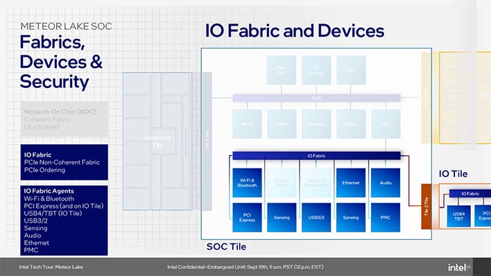 The “South” IO fabric is ordered, but non-coherent and PCIe-based. It is home to Wi-Fi and Bluetooth, PCI Express connections, Sensing, USB 3/2, Ethernet, the Power Management Controller (PMC), and Security controllers. Intel has broken out the Silicon Security Engine from its traditional Converged Security and Manageability Engine (CSME).
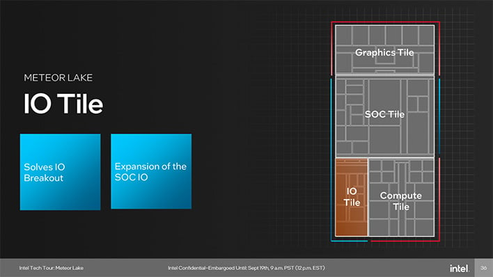 The IO Tile provides additional PCI Express and USB4/Thunderbolt connectivity using the IO fabric. The IO Tile’s positioning alongside the Compute Tile is deliberate, as this configuration effectively extends the surface area of the SOC to make outside connections less crowded.


Breaking up a design into smaller chiplets has its own drawbacks, of course. Packaging it all together becomes a lot more complex, no matter how you slice it. If we disregard 3D V-Cache for a moment, AMD arranges chiplets around each other on a single PCB for its processors, whereas Intel opts to stack silicon directly using its Foveros and Embedded Multi-die Interconnect Bridge (EMIB) technologies. Foveros and EMIB are similar, but distinct advanced packaging techniques that Intel has been using in some products for a few years now.

EMIB debuted first in 2017 in the Stratix 10. This was a field-programmable grid array (FPGA) chip, but the technology has matured into high volume production and is used by Sapphire Rapids today. EMIB uses 55um pitch interconnects to mount die atop the embedded silicon bridge.

Foveros allows for active-on-active “3D” stacking with greater complexity. Foveros was introduced with Lakefield in 2020, where it allowed Intel to layer a compute die with PoP DRAM on top of a base die that is then mounted on the package substrate.


The Compute tile is where most of the processors cores reside. Most you may ask? We’ll get to that. The Compute tile features a mix of the P-cores and E-cores we’re used to from Alder Lake and Raptor Lake, with some microarchitectural improvements. The Compute tile is built using the Intel 4 process node and is actually the only tile in the system directly fabbed by Intel.

The GPU tile is next up. As expected, this contains Intel’s Arc Graphics architecture, specifically Xe-LPG. This is fabbed by TSMC on its N5 process and designed to deliver an approximate 2x performance per watt improvement over the 12th gen Xe graphics. The Graphics tile does not house the Media Engine, though. That has been separated out to reside on the SOC tile, along with the display interfaces.


But there is still much more to cover...
