
But how does a PC decide if an instruction was a floating-point instruction for the 8087 or a regular instruction for the 8086 or 8088 CPU? And how does the 8087 chip interpret instructions to determine what they mean? It turns out that decoding an instruction inside the 8087 is more complicated than you might expect. The 8087 uses multiple techniques, with decoding circuitry spread across the chip. In this blog post, I'll explain how these decoding circuits work.
To reverse-engineer the 8087, I chiseled open the ceramic package of an 8087 chip and took numerous photos of the silicon die with a microscope. The complex patterns on the die are formed by its metal wiring, as well as the polysilicon and silicon underneath. The bottom half of the chip is the "datapath", the circuitry that performs calculations on 80-bit floating point values. At the left of the datapath, a constant ROM holds important constants such as π. At the right are the eight registers that the programmer uses to hold floating-point values; in an unusual design decision, these registers are arranged as a stack. Floating-point numbers cover a huge range by representing numbers with a fractional part and an exponent; the 8087 has separate circuitry to process the fractional part and the exponent.
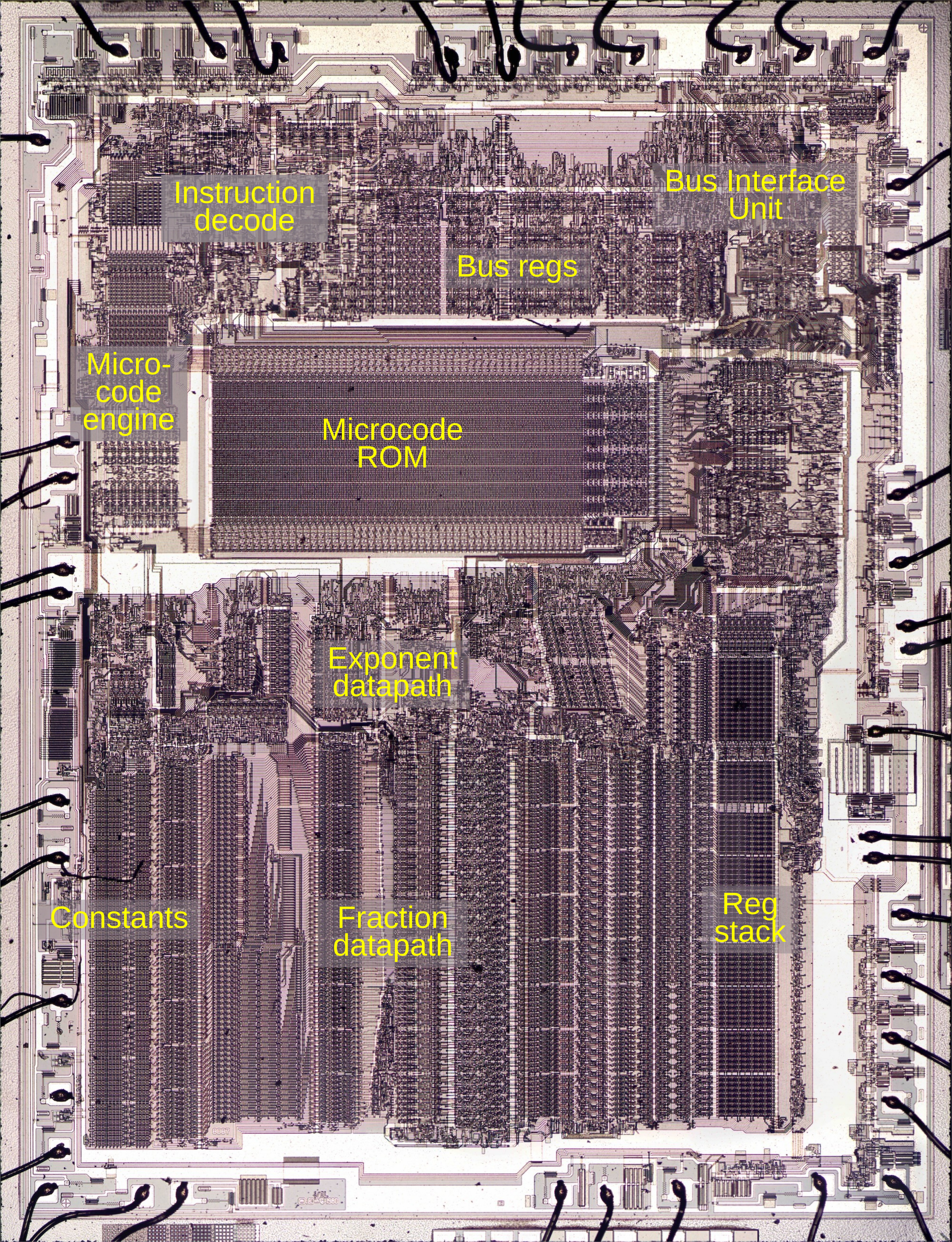
Die of the Intel 8087 floating point unit chip, with main functional blocks labeled. The die is 5 mm×6 mm. Click this image (or any others) for a larger image.
The chip's instructions are defined by the large microcode ROM in the middle.1 To execute an instruction, the 8087 decodes the instruction and the microcode engine starts executing the appropriate micro-instructions from the microcode ROM. In the upper right part of the chip, the Bus Interface Unit (BIU) communicates with the main processor and memory over the computer's bus. For the most part, the BIU and the rest of the chip operate independently, but as we will see, the BIU plays important roles in instruction decoding and execution.
Cooperation with the main 8086/8088 processor
The 8087 chip acted as a coprocessor with the main 8086 (or 8088) processor. When a floating-point instruction was encountered, the 8086 would let the 8087 floating-point chip carry out the floating-point instruction. But how do the 8086 and the 8087 determine which chip executes a particular instruction? You might expect the 8086 to tell the 8087 when it should execute an instruction, but this cooperation turns out to be more complicated.
The 8086 has eight opcodes that are assigned to the coprocessor, called ESCAPE opcodes.
The 8087 determines what instruction the 8086 is executing by watching the bus,
a task performed by the BIU (Bus Interface Unit).2
If the instruction is an ESCAPE, the instruction is intended for the 8087.
However, there's a problem. The 8087 doesn't have any access to the 8086's registers (and vice versa), so the only way
that they can exchange data is through memory.
But the 8086 addresses memory through a complicated scheme involving offsest registers and segment registers.
How can the 8087 determine what memory address to use when it doesn't have access to the registers?
The trick is that when an ESCAPE instruction is encountered,
the 8086 processor starts executing the instruction, even though it is intended for the 8087.
The 8086 computes the memory address that the instruction references and
reads that memory address, but ignores the result.
Meanwhile, the 8087 watches the memory bus to see what address is accessed and stores this address internally in a BIU register.
When the 8087 starts executing the instruction, it uses the address from the 8086 to read and write
memory.
In effect, the 8087 offloads address computation to the 8086 processor.
The structure of 8087 instructions
To understand the 8087's instructions, we need to take a closer look at the structure of 8086 instructions. In particular, something called the ModR/M byte is important since all 8087 instructions use it.
The 8086 uses a complex system of opcodes with a mixture of single-byte opcodes, prefix bytes, and longer instructions. About a quarter of the opcodes use a second byte, called ModR/M, that specifies the registers and/or memory address to use through a complicated encoding. For instance, the memory address can be computed by adding the BX and SI registers, or from the BP register plus a two-byte offset. The first two bits of the ModR/M byte are the "MOD" bits. For a memory access, the MOD bits indicate how many address displacement bytes follow the ModR/M byte (0, 1, or 2), while the "R/M" bits specify how the address is computed. A MOD value of 3, however, indicates that the instruction operates on registers and does not access memory.
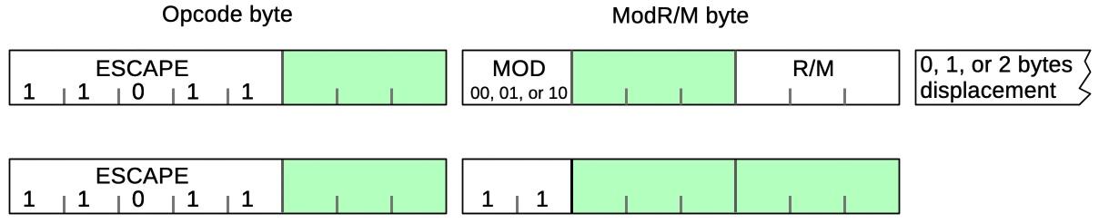
Structure of an 8087 instruction
The diagram above shows how an 8087 instruction consists of an ESCAPE opcode, followed by
a ModR/M byte.
An ESCAPE opcode is indicated by the special bit pattern 11011, leaving three bits (green) available
in the first byte to specify the type of 8087 instruction.
As mentioned above, the ModR/M byte has two forms.
The first form performs a memory access; it has MOD bits of 00,01, or 10 and the R/M bits
specify how the memory address is computed. This leaves three bits (green) to specify the address.
The second form operates internally, without a memory access; it has MOD bits of 11.
Since the R/M bits aren't used in the second form, six bits (green) are available in the R/M byte
to specify the instruction.
The challenge for the designers of the 8087 was to fit all the instructions into the available bits
in such a way that decoding is straightforward.
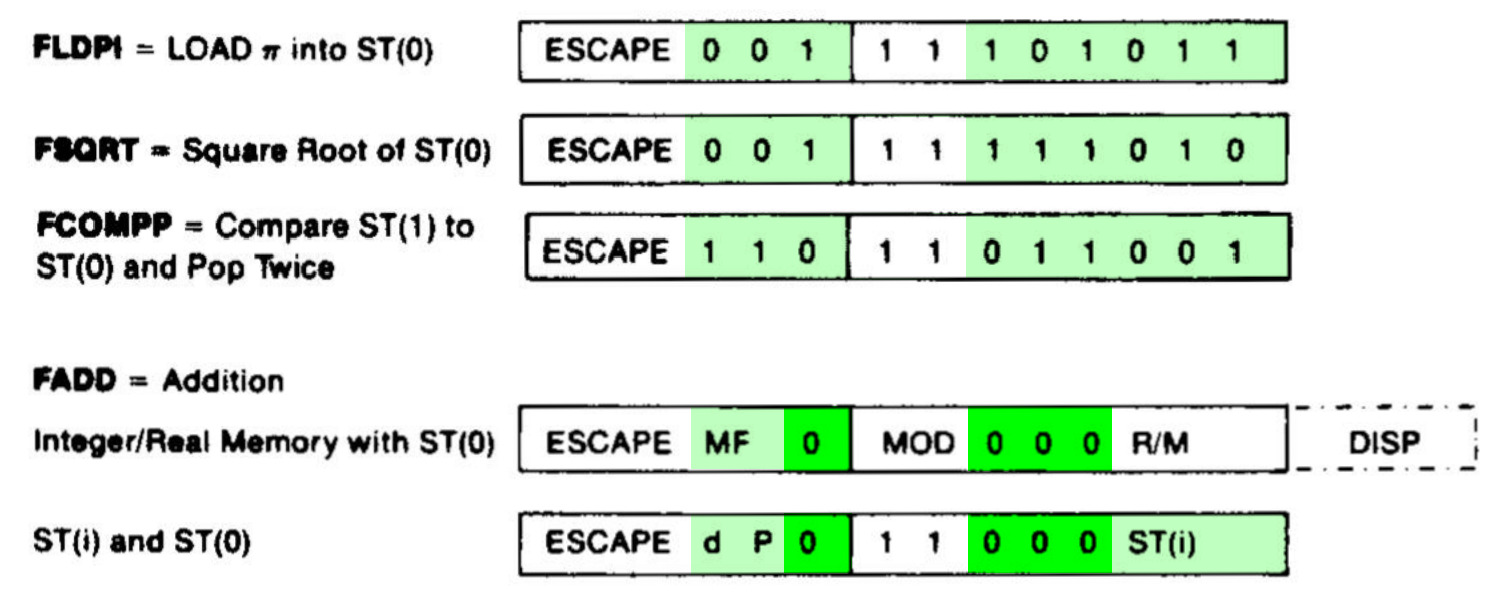
The diagram below shows a few 8087 instructions, illustrating how they achieve this.
The first three instructions operate internally, so they have MOD bits of 11; the green
bits specify the particular instruction.
Addition is more complicated because it can act on memory (first format) or registers (second format), depending on the MOD bits.
The four bits highlighted in bright green (0000) are the same for all ADD instructions;
the subtract, multiplication, and division instructions use the same structure but have
different values for
the dark green bits. For instance, 0001 indicates multiplication and 0100 indicates subtraction.
The other green bits (MF, d, and P) select variants of the addition instruction,
changing the data format, direction, and popping the stack at the end.
The last three bits select the R/M addressing mode for a memory operation, or the stack register
ST(i) for a register operation.
Selecting a microcode routine
Most of the 8087's instructions are implemented in microcode, implementing each step of an instruction in low-level "micro-instructions". The 8087 chip contains a microcode engine; you can think of it as the mini-CPU that controls the 8087 by executing a microcode routine, one micro-instruction at a time. The microcode engine provides an 11-bit micro-address to the ROM, specifying the micro-instruction to execute. Normally, the microcode engine steps through the microcode sequentially, but it also supports conditional jumps and subroutine calls.
But how does the microcode engine know where to start executing the microcode for a particular machine instruction? Conceptually, you could feed the instruction opcode into a ROM that would provide the starting micro-address. However, this would be impractical since you'd need a 2048-word ROM to decode an 11-bit opcode.3 (While a 2K ROM is small nowadays, it was large at the time; the 8087's microcode ROM was a tight fit at just 1648 words.) Instead, the 8087 uses a more efficient (but complicated) instruction decode system constructed from a combination of logic gates and PLAs (Programmable Logic Arrays). This system holds 22 microcode entry points, much more practical than 2048.
Processors often use a circuit called a PLA (Programmable Logic Array) as part of instruction decoding. The idea of a PLA is to provide a dense and flexible way of implementing arbitrary logic functions. Any Boolean logic function can be expressed as a "sum-of-products", a collection of AND terms (products) that are OR'd together (summed). A PLA has a block of circuitry called the AND plane that generates the desired sum terms. The outputs of the AND plane are fed into a second block, the OR plane, which ORs the terms together. Physically, a PLA is implemented as a grid, where each spot in the grid can either have a transistor or not. By changing the transistor pattern, the PLA implements the desired function.
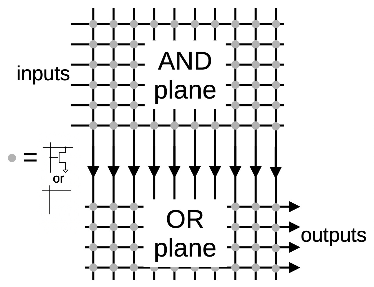
A simplified diagram of a PLA.
A PLA can implement arbitrary logic, but in the 8087, PLAs often act as optimized ROMs.4 The AND plane matches bit patterns,5 selecting an entry from the OR plane, which holds the output values, the micro-address for each routine. The advantage of the PLA over a standard ROM is that one output column can be used for many different inputs, reducing the size.
The image below shows part of the instruction decoding PLA.6 The horizontal input lines are polysilicon wires on top of the silicon. The pinkish regions are doped silicon. When polysilicon crosses doped silicon, it creates a transistor (green). Where there is a gap in the doped silicon, there is no transistor (red). (The output wires run vertically, but are not visible here; I dissolved the metal layer to show the silicon underneath.) If a polysilicon line is energized, it turns on all the transistors in its row, pulling the associated output columns to ground. (If no transistors are turned on, the pull-up transistor pulls the output high.) Thus, the pattern of doped silicon regions creates a grid of transistors in the PLA that implements the desired logic function.7
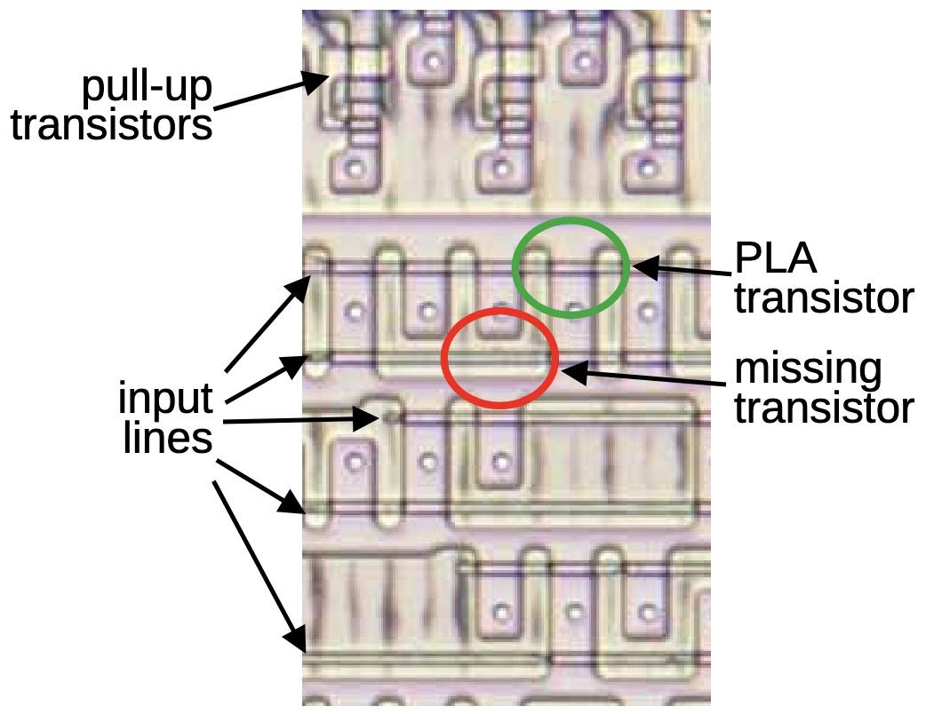
Part of the PLA for instruction decoding.
The standard way to decode instructions with a PLA is to take the instruction bits (and their complements) as inputs.
The PLA can then pattern-match against bit patterns in the instruction.
However, the 8087 also uses some pre-processing to reduce the size of the PLA.
For instance, the MOD bits are processed to generate a signal if the bits are 0, 1, or 2 (i.e.
a memory operation) and a second signal if the bits are 3 (i.e. a register operation).
This allows the 0, 1, and 2 cases to be handled by a single PLA pattern.
Another signal indicates that the top bits are 001 111xxxxx; this indicates that the R/M field
takes part in instruction selection.8
Sometimes a PLA output is fed back in as an input, so a decoded group of instructions can be
excluded from another group.
These techniques all reduce the size of the PLA at the cost of some additional logic gates.
The result of the instruction decoding PLA's AND plane is 22 signals, where each signal corresponds to an instruction or group of instructions with a shared microcode entry point. The lower part of the instruction decoding PLA acts as a ROM that holds the 22 microcode entry points and provides the selected one.9
Instruction decoding inside the microcode
Many 8087 instructions share the same microcode routines. For instance, the addition, subtraction, multiplication, division, reverse subtraction, and reverse division instructions all go to the same microcode routine. This reduces the size of the microcode since these instructions share the microcode that sets up the instruction and handles the result. However, the microcode obviously needs to diverge at some point to perform the specific operation. Moreover, some arithmetic opcodes access the top of the stack, some access an arbitrary location in the stack, some access memory, and some reverse the operands, requiring different microcode actions. How does the microcode do different things for different opcodes while sharing code?
The trick is that the 8087's microcode engine supports conditional subroutine calls, returns, and jumps, based on 49 different
conditions (details).
In particular, fifteen conditions examine the instruction.
Some conditions test specific bit patterns, such as branching if the lowest bit is set, or more complex patterns such as
an opcode matching 0xx 11xxxxxx. Other conditions detect specific instructions such as FMUL.
The result is that the microcode can take different paths for different instructions. For instance, a reverse subtraction or
reverse division is implemented in the microcode by testing the instruction and reversing the arguments if necessary, while sharing the rest of the code.
The microcode also has a special jump target that performs a three-way jump depending on the current machine instruction that is being executed. The microcode engine has a jump ROM that holds 22 entry points for jumps or subroutine calls.10 However, a jump to target 0 uses special circuitry so it will instead jump to target 1 for a multiplication instruction, target 2 for an addition/subtraction, or target 3 for division. This special jump is implemented by gates in the upper right corner of the jump decoder.
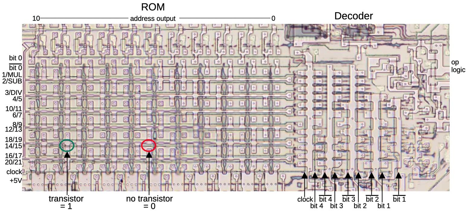
The jump decoder and ROM. Note that the rows are not in numerical order; presumably, this made the layout slightly more compact. Click this image (or any other) for a larger version.
Hardwired instruction handling
Some of the 8087's instructions are implemented directly by hardware in the Bus Interface Unit (BIU), rather than using microcode. For example, instructions to enable or disable interrupts, or to save or restore state are implemented in hardware. The decoding for these instructions is performed by separate circuitry from the instruction decoder described above.
In the first step, a small PLA decodes the top 5 bits of the instruction.
Most importantly, if these bits are 11011, it indicates an ESCAPE instruction, the start of
an 8087 operation. This causes the 8087 to start interpreting the instruction and stores
the opcode in a BIU register for use
by the instruction decoder.
A second small PLA takes the outputs from the top-5 PLA and combines them with the lower three bits.
It decodes specific instruction values:
D9, DB, DD, E0, E1, E2, or E3.
The first three values correspond to specific ESCAPE instructions,
and are recorded in latches.
The two PLAs decode the second byte in the same way. Logic gates combine the PLA outputs from the second byte with the latched values from the first byte, detecting eleven hardwired instructions.11 Some of these instructions operate directly on registers, such as clearing exceptions; the decoded instruction signal goes to the relevant register and modifies it in an ad hoc way. 12. Other hardwired instructions are more complicated, writing chip state to memory or reading chip state from memory. These instructions require multiple memory operations, controlled by the Bus Interface Unit's state machine. Each of these instructions has a flip-flop that is triggered by the decoded instruction to keep track of which instruction is active.
For the instructions that save and restore the 8087's state (FSAVE and FRSTOR), there's one more complication.
These instructions are partially implemented in the BIU, which moves the relevant BIU registers to or from memory.
But then, instruction processing switches to microcode, where a microcode routine saves
or loads the floating-point registers. Jumping to the microcode routine is not implemented through the regular microcode jump circuitry.
Instead, two hardcoded values force the microcode address to the save or restore routine.13
Constants
The 8087 has seven instructions to load floating-point constants such as π, 1, or log10(2). The 8087 has a constant ROM that holds these constants, as well as constants for transcendental operations. You might expect that the 8087 simply loads the specified constant from the constant ROM, using the instruction to select the desired constant. However, the process is much more complicated.14
Looking at the instruction decode ROM shows that different constants are implemented with different
microcode routines: the constant-loading instructions FLDLG2 and FLDLN2 have one entry
point; FLD1, FLD2E, FLDL2T, and FLDPI have a second entry point, and FLDZ (zero) has a third entry point.
It's understandable that zero is a special case, but why are there two routines for the other constants?
The explanation is that the fraction part of each constant is stored in the constant ROM, but the exponent is stored in a separate, smaller ROM. To reduce the size of the exponent ROM, only some of the necessary exponents are stored. If a constant needs an exponent one larger than a value in the ROM, the microcode adds one to the exponent ROM value, computing the exponent on the fly.
Thus, the load-constant instructions use three separate instruction decoding mechanisms. First, the instruction decode ROM determines the appropriate microcode routine for the constant instruction, as before. Then, the constant PLA decodes the instruction to select the appropriate constant. Finally, the microcode routine tests the bottom bit of the instruction and increments the exponent if necessary.
Conclusions
To wrap up the discussion of the decoding circuitry, the diagram below shows how the different circuits are arranged on the die. This image shows the upper-right part of the die; the microcode engine is at the left and part of the ROM is at the bottom.
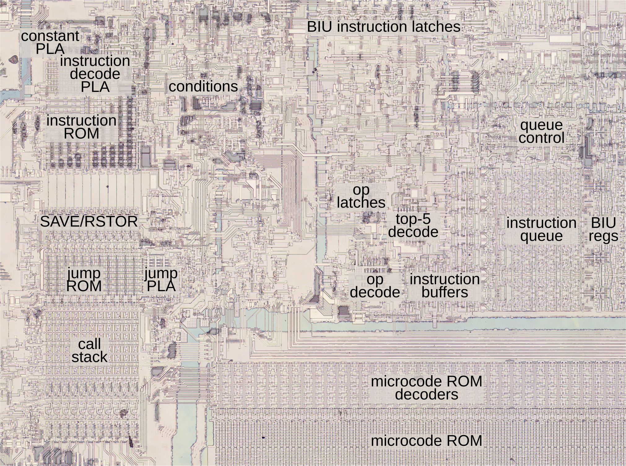
The upper-left portion of the 8087 die, with functional blocks labeled.
The 8087 doesn't have a clean architecture, but instead is full of ad hoc circuits and corner cases. The 8087's instruction decoding is an example of this. Decoding is complicated to start with due to the 8086's convoluted instruction formats and the ModR/M byte. On top of that, the 8087's instruction decoding has multiple layers: the instruction decode PLA, microcode conditional jumps that depend on the instruction, a special jump target that depends on the instruction, constants selected based on the instruction, and instructions decoded by the BIU.
The 8087 has a reason for this complicated architecture: at the time, the chip was on the edge of what was possible, so the designers needed to use whatever techniques they could to reduce the size of the chip. If implementing a corner case could shave a few transistors off the chip or make the microcode ROM slightly smaller, the corner case was worthwhile. Even so, the 8087 was barely manufacturable at first; early yield was just two working chips per silicon wafer. Despite this difficult start, a floating-point standard based on the 8087 is now part of almost every processor.
Thanks to the members of the "Opcode Collective" for their contributions, especially Smartest Blob and Gloriouscow.
For updates, follow me on Bluesky (@righto.com), Mastodon (@[email protected]), or RSS.
